In the literal translation of the chipset (chipset) means "chipset". The chipset, which is also called a set of system logic, is one or more of two chips (chips) intended for organizing interaction between the processor, memory, I / O ports and the other components of the computer. At the dawn of the development of computer equipment, dozens of individual chips were used to organize interaction between individual elements of PCs, which, of course, was extremely uncomfortable. And only with the advent of the I486 processor, individual chips began to combine into one or two large chips, which received the name of the chipset.
The creation of the PCI bus, individual chipset chips began to call bridges - so there were well-established terms: the North Bridge (North Bridge) and the South Bridge (South Bridge) of the chipset, while the north bridge is connected directly to the processor, and the South-Northern. In some cases, manufacturers combine the northern and southern bridge into one microcircuit, and such a solution is called one-chip, and if two chips are, then this is a two-seater.
The northern bridge of the chipset traditionally includes a memory controller (with the exception of processor chipsets with AMD64 architecture), a graphic bus controller (AGP or PCI Express X16), an interface of interaction with the southern bridge and the interface of interaction with the processor. In some cases, the northern bridge of the chipset may contain additional PCI Express X1 lines for organizing interaction with expansion cards that have an appropriate interface.
The south bridge of the chipset is the function of organizing interaction with I / O devices. The southern bridge contains hard drive controllers (SATA and / or PATA), a USB controller, a network controller (MAC-level only), a PCI bus controller and PCI-Express bus, an interrupt controller and a DMA controller. In addition, the South Bridge is usually embedded with a sound controller, and in this case the codec chipset is still needed to the chipset. In addition, the South Bridge is connected with two more important chips on the motherboard: BIOS ROM microcircuit and Super I / O microcircuit responsible for serial and parallel ports and for floppy disk drive.
To connect the northern and southern bridges with each other, a special dedicated tire is used, and different manufacturers use different tires for this (with different bandwidth):
- Intel - Dmi (DIRECT MEDIA INTERFACE),
- ULI - Hypertransport;
- VIA - V-LINK;
- SIS - Mutiol;
- ATI - Hypertransport, PCI Express;
- NVIDIA - Hypertransport.
As a rule, the name of the chipset coincides with the name of the Northern Bridge, although it is more correct to indicate that the totals of the Northern and South Bridges are more correct, since in many cases the same northern bridge of chipset can be combined with various options for southern bridges.
The chipset is the basis of any motherboard. In fact, the motherboard functionality and its performance 90% are determined by the chipset, on which the supported processor type depend on the type of memory, as well as the functionality of connecting peripheral devices.
Chipset selection is very large for today. And if the processors have been producing only two companies: Intel and AMD, then chipsets are produced by Intel, Via, and Sis, and NVIDIA, and ATI, and ULI.
Intel's chipsets
intel provides a very diverse range of chipsets for Intel Pentium D processors, Intel Pentium 4 and Intel Celeron D. And if we talk about the modern Intel's chipsets, then start with the Intel 915 Express family.
Intel 915/925 Express Chipset Family
The Intel 915/925 Express family of chipsets (Table 1) has several characteristic features.
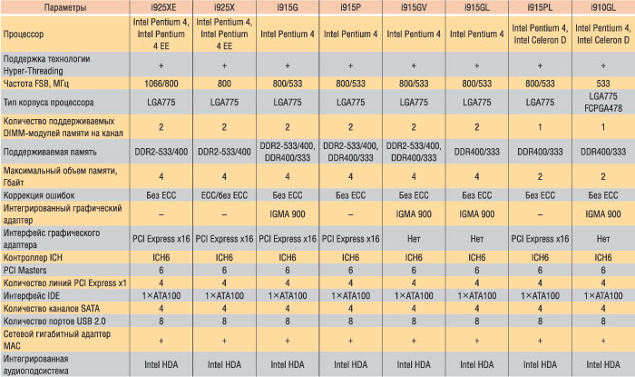
First of all, new chipsets are focused on supporting Intel Pentium 4 (Prescott) processors in the new LGA775 building, which means the availability of a new connector on motherboards and the impossibility of using older versions of processors designed for Socket 478 connector. Another important point is that new chipsets (True, not all) are focused on supporting a new type of DDR2-533 / 400 memory. Intel Flex Memory technology allows you to work with memory in both single-channel and two-channel mode. The third important point is the support of the new PCI Express tire. In the new generation of motherboards, the PCI Express X16 slot is envisaged for the video card.
In addition, a number of models of the Intel 915/925 Express family has an integrated Intel Graphic Media Accelerator 900 graphics controller (IGMA 900).
The Northern Bridge of Intel 915/925 EXPRESS chipsets is associated with a high-speed DMI tire (Direct Media Interface), which is a modified version of PCI Express X4 (~ 2 GB / s), with an I / O hub (southern bridge) ICH6. In total, there are three types of southern bridge: ICH6R (chip 82801FR), ICH6W (80801FW) and ICH6RW (80801RW).
The new version of the southern bridge has a number of significant advantages compared to the previous version of ICH5, namely:
- new 8-channel sound Intel High Definition Audio (Intel HD Audio);
- eight USB 2.0 ports;
- tire PCI Express X1;
- tire PCI;
- four SATA channels;
- one PATA channel;
- intel Wireless Connect Technology;
- network gigabit interface Intel GBE.
Let's start with the new sound of Intel HD Audio, also known as Azalia codenamed. This joint development of Dolby Laboratories and Intel supports 8-channel sound (format 7.1) and provides 24-bit coding at 192-kHz sampling frequency, which guarantees high sound quality. In addition, Intel HD Audio works with all new audio formats: Dolby, DTS, DVD-Audio.
An important feature of the new South South Bridge ICH6 is the support of the PCI Express X1 tire, which provides bandwidth up to 500 MB / s. In addition, this tire supports bilateral traffic and has smaller delays. All Intel 915/925 Express family chipsets support up to four PCI Express X1 channels.
The South Bridge ICH6 has a built-in four-channel SATA controller, and if it is a version of the southern ICh6R or ICH6RW bridge, then the SATA RAID controller is supported on all four channels. It is possible to organize RAID arrays of levels 0, 1 or 0 + 1. SATA RAID controller integrated into the southern bridge of the chipset supports command routing technology (Native Command Queuing, NCQ), which allows to reduce delays, and consequently, increase productivity.
In addition, the SATA RAID controller supports the possibility of hot disk connection and auto-installation function.
And the last feature on which we would like to pay attention is the Intel Wireless Connect technology, which is implemented in the versions of the South Bridge ICH6W and ICH6RW. In fact, the South Bridge is integrated with a wireless access point and a wireless network adapter that meets the IEEE 802.11 b / g standard. In this case, the PC can be configured both as a client device, and as an access point.
Intel 910gl Express
Intel 910GL Express chipset is designed for massive and inexpensive office PCs. According to the functionality, it can be attributed to the family of Intel 915 chipsets, which will be discussed further, and thus consider it as a "younger" model of the chipsets of the Intel 915 family.
Intel 910GL Express supports Intel Pentium 4 (Prescott) and Intel Celer D with Hyper-Threading technology, and its distinctive feature is support for the system tire with a frequency of only 533 MHz (tire throughput is 4.2 GB / s). Consequently, the optimal is the combination of this chipset with the Intel Celeron D. processor.
Intel 910GL Express Chipset Memory Controller (82910GL GMCH chip) is two-channel and provides DDR333 and DDR400 memory (PC3100 / 2700 SDRAM)
Total chipset supports up to 2 GB of memory - 1 GB for each channel. At the same time in each of the channels to install the memory modules is provided by one DIMM slot. That is why the Intel 910GL EXPRESS chipset finds use exclusively in motherboards with the MicroATX formator.
The memory controller allows you to use non-buffered 64-bit memory without ECC error correction.
Since the chipset is focused on budget office solutions, then it integrated Intel Graphic Media Accelerator 900 (IGMA 900) graphics controller (IGMA 900), and the interface for installing an external graphics card is not provided.
Intel 915PL Express
Intel 915PL Express chipset, intended for mass and inexpensive office PCs, is largely similar to the Intel 910GL Express chipset, but there are a number of nuances that allow you to talk about higher performance of the Intel 915PL Express chipset. First of all, the Intel 915PL EXPRESS chipset supports Intel Pentium 4 (Prescott) and Intel Celeron D processors with Hyper-Threading technology. In contrast to the Intel 910GL Express chipset, in addition to supporting the system bus with a frequency of 533 MHz, the frequency of the 800 MHz system bus is maintained. Thus, the best combination of this chipset with the Intel Pentium 4 processor (PRESCOTT) will be the best.
Intel 915PL EXPRESS chipset memory controller is two-channel and provides DDR333 and DDR400 memory (PC3100 / 2700 SDRAM).
The chipset supports up to 2 GB of memory, that is, 1 GB per channel for each channel, and in each of the channels to install the memory modules, there is one DIMM slot. As a result, Intel 915PL Express, as previously reviewed by the Intel 910GL EXPRESS chipset, finds use exclusively in motherboards with Microatx form factor.
Unlike Intel 910GL Express, there is no integrated graphics controller in the 915PL EXPRESS chipset, and there is a PCI Express X16 bus to install an external graphics card.
Intel 915GL Express
Intel 915GL EXPRESS chipset, focused on massive and inexpensive office PCs, is largely similar to the Intel 910GL Express chipset and is designed for Intel Pentium 4 (Prescott) processors and Intel Celeron D with Hyper-Threading technology, LGA775 enclosure and system tire frequency 533 and 800 MHz.
The memory controller of this chipset is two-channel and provides operation with the memory DDR333 and DDR400 (PC3100 / 2700 SDRAM). The chipset supports up to 4 GB of memory - 2 GB per channel, and in each of these channels to install the memory modules there are two DIMM slots. Actually, if you do not consider the support of the frequency of the 800 MHz system tire, it is precisely the main difference between this chipset from Intel 910GL Express. Otherwise, this model completely repeats the Intel 910GL EXPRESS chipset.
Intel 915GV Express
Intel 915GV Express, like all the Intel 915/925 Express chipsets considered above, is intended for low-cost mass PCs, however, in contrast to the discussed chipsets, Intel 915GV Express is focused on the Intel Pentium 4 processor with Hyper-Threading technology and with the system tire frequency 533 and 800 MHz.
The memory controller of this chipset is two-channel and provides work with both DDR333 and DDR400 and DDR400 and DDR2-533 and DDR2-400 memory. Total chipset supports up to 4 GB of memory, that is, 2 GB for each channel. At the same time, in each of the channels for the installation of memory modules, two DIMM slots are provided.
The rest of the Intel 915GV EXPRESS chipset completely repeats the Intel 915GL Express model. Thus, the Intel Graphic Media Accelerator 900 (IGMA 900) graphic controller is integrated here, but there is no interface to install an external graphics card.
Intel 915p Express
Intel 915P Express chipsets almost completely repeats Intel 915GV Express, in one exception - there is no built-in graphic controller here, and instead of it to install an external graphics card, the PCI EXPRESS X16 interface is provided. In all the rest of the Intel 915P Express and Intel 915GV Express chipsets are identical.
Intel 915G Express
Intel 915G Express is the most functional and respectively expensive in the line of Intel 915 chipsets.
The only difference in this chipset from Intel 915p Express is that the IGMA 900 graphic controller is integrated into Intel 915G Express, and the PCI Express X16 interface is provided to install an external graphics card. In all other, the Intel 915G Express and Intel 915P Express chipsets are exactly the same.
Intel 925x Express
Intel 925x Express is focused on creating mass, but high-performance PCs. This chipset supports the Intel Pentium 4 (Prescott) processor, made according to 90 nanometer technology, and the frequency of the system tire is 800 MHz. Accordingly, the maximum bandwidth of the system tire is 6.4 GB / s. Intel 925x Express chipset is designed for Intel Pentium 4 and Intel Pentium 4 Extreme Edition processors, and therefore the frequency of the 533 MHz system bus is not provided there.
The chipset memory controller (MCH) is two-channel and supports only the new DDR2-533 / 400 memory. When using DDR2-533 memory in two-channel mode, the maximum bandwidth of the memory bus is 8.5 GB / s.
In total, the memory controller in accordance with the specification supports up to 4 GB of memory and four DIMM slots (two each channel). Note that, unlike all other chipsets of the Intel 915/925 Express family, Intel 925x Express memory supports work with ECC memory.
Since this chipset is intended for productive PCs, there is no integrated graphics controller IGMA 900, and the PCI Express X16 interface to install an external graphics card, naturally, is available.
Intel 925xe Express.
The 1066 MHz system tire frequency support, implemented in the Intel Pentium 4 Extreme Edition processor, required and the use of a new chipset, or rather a new revision of the already-known Intel 925x Express chipset, which was called Intel 925xe Express. In fact, the only distinguishing property of the new version of the chipset is to support the new FSB frequency - 1066 MHz. All other characteristics of Intel 925xe Express have not changed, except that the controller of its memory does not support ECC memory.
The memory controller of this chipset supports the memory DDR2-533 in two-channel mode, and the memory bus has a bandwidth of 8.5 GB / s.
If in the Intel 925X Express chipset, the processor tire has a 6.4 GB bandwidth (800 MHz64 bits \u003d 6.4 GB / s), which makes it not completely balanced from the memory bus, then in Intel 925xe Express, the processor tire has a bandwidth 8.5 GB / s (1066 MHzѕ64 bits \u003d 8.5 GB / s), that is, in this sense it is fully balanced from the memory bus.
But, in addition to balanced by the bandwidth of the memory tire and the processor bus, this model has another advantage - the transition to the frequency of the system tire (support frequency) in 266 MHz. The fact is that in this case the memory DDR2-533 works in synchronous with a processor bus mode, which minimizes the data transfer delays to the memory controller.
Intel 945/955 Express Chipset Family
Compared to revolutionary changes in the possibilities of desktop platforms that provided intel 915/925 EXPRESS chipsets, a new family of Intel 945/955 Express chipsets (Table 2) is rather a logical development of the Intel 915/925 Express family than something fundamentally new .
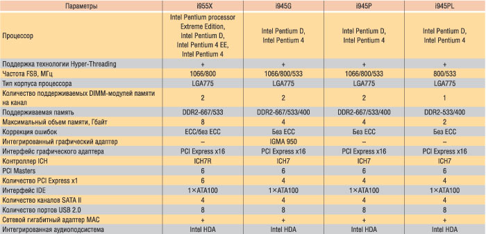
Small improvements touched, in fact, only supporting the high speeds of interfaces and support new intel dual-core processors. Minor changes have been undergoing the southern bridge of chipset: in this family, the ICH7 or ICH7R I / O hub is used as a southern bridge, which is associated with the North Bridge on the DMI bus, which has a bandwidth of 2 GB / s.
The main difference of the new southern bridge from the former version of ICH6 is to support the new SATA II standard (second generation of the standard) with a 300 MB / s bandwidth. Thus, the South Bridge ICH7 supports four SATA II channels with AHCI support and NCQ functions. The ICH7R version allows you to organize a RAID-array levels 0, 1, 0 + 1 (10) and 5 of SATA disks.
Another small difference between ICH7 and ICH6 is that the southern ICH7R bridge supports six PCI Express X1 channels, while the South Bridge ICH7 supports only four channels. The rest of the South Bridge in Ich7 is no different from that in ICH6.
Intel 945PL Express
Intel 945PL Express - the younger model in the Intel 945/955 Express chipset family, focused on the support of dual-core processors of the Intel Pentium D family and single-core processors of the Intel Pentium family 4. A distinctive feature of this chipset is the support of the system tire frequency 800 and 533 MHz. In addition, the two-channel memory controller supports operation only with the memory of DDR2-533 and DDR2-400 with a maximum amount of up to 2 GB, and only two DIMM slots are provided to install the memory modules - one by one on the channel.
The chipset does not have an embedded graphics controller, and the PCI Express X16 interface is provided to install an external graphics card.
Intel 945p Express
Intel 945P Express chipset differs from the previous one, except the frequencies of the system bus 80 and 533 MHz, support for the system tire frequency 1066 MHz is implemented. In addition, the two-channel memory controller supports the operation not only with the memory DDR2-533 and DDR2-400, but also with the memory DDR2-667 with a maximum amount of up to 4 GB, moreover, four DIMM slots are already for the installation of memory modules, that is, Two on the canal. In the rest of the Intel 945P Express is similar to the Intel 945PL Express chipset.
Intel 945g Express.
The Intel 945G Express model differs from Intel 945P Express only by the presence of an embedded graphics controller IGMA 950 (the PCI Express X16 interface is also present). Compared with the previous version of the integrated graphics controller IGMA 900, the new version has a number of improvements. In particular, the clock frequency of the nucleus (400 versus 333 MHz) is increased. Accordingly, the speed of filling the textures (1.6 GT / C against 1.3 GT / s). And the use of DDR2-667 memory allows you to increase the maximum video memory bandwidth to 10.6 GB / s.
The remaining parameters of the Intel 945G Express chipset are identical to Intel 945P Express.
Intel 955x Express
Intel 955x Express chipset is the older model in the Intel 945/955 Express chipset family and is designed for high-performance PCs and graphics stations. Unlike all other chipsets of this family, it is focused on using the Intel Pentium Processor Extreme Edition 840 dual-core processor, dual-core processors of the Intel Pentium D family, single-core processors of the Intel Pentium 4 Extreme Edition family and conventional Intel Pentium 4 family processors.
This chipset supports the frequency of the system bus 1066 and 800 MHz (frequency 533 MHz specification is not provided). In addition, the memory controller of this chipset supports operation only with DDR2-667 and DDR2-533 memory with a maximum up to 8 GB (supported operation with ECC memory). In the rest, this chipset is the same as Intel 945P Express.
NVIDIA chipsets
NVIDIA's assortment has quite a lot of chipsets - both for AMD processors and Intel processors. However, the confusion in NVIDIA chipsets, too, a lot, which is primarily promoted by NVIDIA. There is practically no technical information on the company's website, and there is simply no mention of some chipsets there.
The story about the modern model range of NVIDIA chipsets can be started with the NVIDIA NForce4 chipsets family.
NVIDIA NForce4 family chipsets
NVIDIA NForce4 chipsets (Table 3) came to replace the NVIDIA NForce3 chipset family and differs from them higher functionality. The distinctive feature is the support of the PCI Express bus. The NVIDIA NForce4 chipset family includes four models: NVIDIA NFORCE4, NVIDIA NForce4 SLI, NVIDIA NForce4 Ultra, NVIDIA NForce4 SLI Intel Edition.
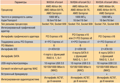
The functionality and characteristics of the chipsets of the NVIDIA NForce4 family (with the exception of NVIDIA NForce4 SLI Intel Edition) are close to each other, and their differences are minimal. Thus, the Hypertransport bus frequency for all chipsets of the NVIDIA NForce4 family is 1000 MHz, and the bit rate is 16 bits (symmetric bus), which, of course, is more than enough for modern AMD processors. Another general characteristic of all chipsets of this family is the support of the PCI Express X16 tire.
The NForce4 SLI chipset additionally allows you to use two NVIDIA video cards in SLI mode. To do this, the chipset distributes the PCI Express X16 bus lines into two PCI Express X8 tires (respectively, on motherboards there are two slots for installing video cards), and the rest provides video cards and their drivers.
The NVIDIA NForce4 family chipsets also support four PCI Express X1 channels, that is, there are 20 PCI Express X1 channels (including PCI Express X16). And the number of USB 2.0 ports increased to 10. In addition to the traditional two-channel interface of ATA133, there is a four-channel SATA controller in the NVIDIA NForce4 family chipsets, and it is possible to merge into the RAID array disk with different interfaces.
The difference between the chipsets of this family is that the NVIDIA NForce4 chipset uses a conventional SATA controller (150 Mbps), and in NVIDIA NForce4 SLI / ULTRA chipsets - the SATA II controller (300 Mbps) with a hot-swap function and With support for reordering NCQ commands (Native Command Queuing).
In the chipsets of the NVIDIA NForce4 family, the Gigabit Ethernet controller (MAC level) is integrated, and in NVIDIA NForce4 SLI / ULTRA models, the network controller is supplemented with a software and hardware firewall function with a hardware accelerator for processing ActiveArmor network packets.
In all the chipsets of the NVIDIA NForce4 family, the audio controller was upgraded: the AC'97 codecs are used, and the number of S / PDIF channels doubled, besides added support for the sampling frequency of 96 kHz, other changes have been added. True, the hardware processing of the sound controller does not fulfill.
NVIDIA NFORCE4 SLI Intel Edition
Although formally, the NVIDIA NForce4 SLI Intel Edition chipset and refers to the NForce4 family, it differs dramatically from all other models of this family. As follows from the title, this chipset is focused on Intel processors, and in addition, supports SLI mode. Note that at the moment it is the only chipset with full support for SLI mode for Intel processors. And although there are options for motherboards based on chipsets of the Intel 945/955 Express family with two PCI Express X16 slots that support the simultaneous operation of two video cards, but it is not necessary to talk about the full SLI mode in this case. The fact is that in the specified motherboards in reality one slot uses the PCI Express X16 bus, and the second - PCI Express X4 by combining four PCI Express X1 lines. Thus, we are talking about asymmetric configuration bandwidth, and if the first video card, utilizes the PCI Express X16 bus, directly communicates with the North Bridge, then the second video card, utilizing the PCI Express X4 bus, communicates with the North Bridge through the South. And if you remember that the South Bridge is associated with the Northern DMI bus with a 2 GB bandwidth / s and that the bandwidth of the PCI Express X4 interface is also 2 GB / s, it becomes clear that a smaller bandwidth is valid for the share of the second video card, The even interface bandwidth. It is clear that to name this mode of operation by the SLI mode, only with a large stretch.
As in the case of the NVIDIA NForce4 SLI chipset version for AMD 64 processors, the NVIDIA NForce4 SLI Edition chipset is focused on using in the most high-performance gaming PCs and graphics stations to work with three-dimensional graphics. The main thing that distinguishes it from all other NVIDIA chipsets is a two-way diagram. NFORCE4 SLI Intel Edition, called System Platform Processor (SPP), combines a two-channel DDR2 memory controller, a processor interaction interface, a PCI Express bus controller and an interaction interface with a southern bridge. The south bridge, called Media and Communication Processor (MCP), is essentially an I / O hub.
The connection between SPP and MCP is provided with the Hypertransport bus with a frequency of 800 MHz and with a 1,6 GB bandwidth / s in each direction.
The NForce4 SLI Intel Edition chipset allows you to use any Intel processor with the LGA775 connector and the FSB 533, 800 and 1066 MHz frequency. In addition, the chipset supports Hyper-Threading technology. The chipset memory controller allows you to use DDR2-400 / 533/667 memory in two-channel operation mode.
An important feature of the NForce4 SLI Intel Edition memory controller is that it has a dedicated address of the addresses and commands for each of the memory modules, and this leads to a reduction in the load on each of these tires twice, which ultimately reduces the response time of the memory modules to the command Controller. The memory controller supports 1T Memory Timing mode, so that the memory modules receive commands and addresses during the same tact during which they were transmitted from the controller. Chipsets that do not use the dedicated address bus and commands for each of the modules are often forced to operate in 2T Memory Timing mode, which is necessary at high loading of this bus. In such mode, the addresses and commands are understood by memory modules only on the next clock after their feed.
In addition, in the memory controller used in the NForce4 SLI Intel Edition, a specialized DASP processor is used (Dynamic Adaptive Speculative Preprocessor) version 3.0. This processor provides a preliminary sample from the memory of those data that may be requested by the central processor in the near future, which reduces the downtime of the central processor caused by the absence of data for processing. DASP 3.0 processor supports Hyper-Threading technology and Intel dual-core processors, that is, knows how to recognize access to each of the kernels (physical or logical).
As for the other functionality of the NVIDIA NForce4 SLI Intel Edition chipset, they are completely similar to the capabilities of the NVIDIA NForce4 SLI chipset for AMD64 processors. SLI mode is achieved by using two PCI Express X8 tires. Like the NVIDIA NForce4 chipset, the NForce4 SLI Intel Edition model has a two-channel ATA133 controller and two dual-channel SATA II controllers with NCQ support and with the possibility of hot disk connection. In addition, it is possible to combine levels 0, 1, 0 + 1 and 5 discs with different interfaces in RAID arrays.
Of course, in the NVIDIA NForce4 SLI Intel Edition chipset, as in NVIDIA NForce4 SLI, an integrated gigabit network controller with a built-in ActiveArmor network security feature.
NVIDIA GeForce 6100 IGP Chipsets Family
In September of this year, NVIDIA has expanded the AMD Athlon 64 and Sempron model range of chipsets, representing the C51 code name chipset, which includes a GeForce 61xx IGP graphics processor (based on the GeForce 6 engine) and a media component processor (MCP) of the NForce 400 series.
Two versions of the graphics processor are currently available - GeForce 6100 IGP and GeForce 6150 IGP, as well as two versions of the MCP processor - NFORCE 410 and NFORCE 430, and three combinations of the combination of IGP- and MCP processors are possible: GeForce 6150 IGP / NForce 430, GeForce 6100 IGP / NForce 430, GeForce 6100 IGP / NForce 410.
The GEFORCE 61XX IGP series processors for communication with the central processor use the Hypertransport bus with a clock frequency of 2000 MHz, and for communication with MCP processors - the Hypertransport bus with a clock frequency of 1600 MHz. In addition, the GEFORCE 61XX IGP series processors have the PCI Express X16 interface to install an external video card, and also support PCI Express X1 lines - the GEFORCE 6150 processor has two such lines, and GeForce 6100 IGP is one.
The GEFORCE 61XX IGP graphics processor supports the DirectX 9.0c API (version 3.0 shaders). The difference between GeForce 6100 IGP and GeForce 6150 IGP is that the GEFORCE 6150 GEFORCE core operates on a clock frequency of 475 MHz, and the GEFORCE 6100 IGP graphics core is 425 MHz. In addition, the TV encoder is present in the GeForce 6150 kernel, and there is no IGP in the GeForce 6100 kernel. Detailed technical characteristics of GEFORCE 61XX IGP processors are displayed in Table. four.
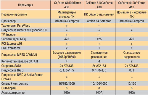
NForce 4xx MCP processors support Intel High Definition Audio audio controller and have built-in SATA II controllers with the ability to combine disks in RAID arrays. The difference between the NForce 410 and NForce 430 is that the NForce 410 MCP processor uses a two-channel SATA II controller, and the NForce 430 is four-channel. In addition, a gigabit network interface is present in the NForce 430 version.
Of the technical characteristics of the chipsets presented in Table. 4, apparently appoint each of three modifications: option GeForce 6150 / NForce 430 Designed for multimedia computers, GeForce 6100 / Nforce 430 - for a general purpose PC, GeForce 6100 / NForce 410 - For office or budget PCs. Combination GeForce 6150 / NForce 430 It can become an excellent basis for Tivo television consoles or multimedia PCs running Windows Media Center with high-definition television support and high-quality sound.
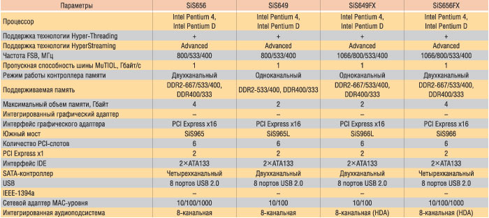
The SIS656 chipset supports the PCI Express X16 bus, which allows you to consider it as a basis for building modern high-performance PCs. In addition, a two-channel DDR2 memory controller is integrated into the northern bridge of the SIS656 chipset, which provides operation with DDR2-667 / 533/400 memory. In addition to this, the chipset supports work and with memory DDR400 / 333/266. The maximum amount of memory that can be set to the system is 4 GB.
The supported FSB frequency is 800/533/400 MHz, that is, the chipset supports Intel Pentium 4 processors with Hyper-Threading technology and dual-core processors of the Intel Pentium Dual family.
The North Bridge of the SIS656 chipset is associated with the southern bridge - the SIS965 chip - on the Mutiol bus with 1 GB / s bandwidth.
In the SIIS965 south bridge, in addition to traditional functions (two-channel ATA133 controller, eight USB 2.0 ports, 8-channel sound, six PCI slots), there is a four-channel SATA controller with the possibility of combining disks in the RAID array of levels 0, 1 and 0+ one. In addition, a two-channel PCI Express X1 controller and a gigabit network controller (MAC level) are integrated into the southern bridge.
The SIS649 chipset model, the northern bridge of which is used together with the SIS965L south bridge, is a kind of lightweight, trimmed version of SIS965. It follows that this chipset is focused on budgetary-level budget solutions.
The North Bridge supports the FSB 800/533/400 MHz frequency, therefore, the chipset supports Intel Pentium 4 processors with Hyper-Threading technology and dual-core processors of the Intel Pentium Dual family.
As in the SIS656 chipset, the PCI Express X16 bus is supported for setting the video card. Actually, the only difference between the northern bridges of SIS649 and Sis656 chipset is that the Sis649 uses a single-channel memory controller. This supports DDR2-533 / 400 memory, as well as the memory DDR400 / 333 with a maximum volume of up to 2 GB.
South Bridge SIS965L is also a lightweight version of the SIS965 bridge. The only difference is that a two-channel is used, and not a four-channel SATA controller and that there is no gigabit network controller (MAC-level).
Sis649fx
SIS649FX is an improved version of the SIS649 chipset, although the improvements of the northern bridge is only two. First, the FSB frequency support is added to 1066 MHz, and secondly, a single-channel memory controller supports DDR2-667 memory. In the rest ofstairs, the northern bridge of the SIS649FX chipset is completely repeated by the SIS649 model.
As a south bridge in the SIS649FX chipset, the SIS966L chip is used, but it differs from the south SIS965L bridge in one detail: 8-channel audio controller High Definition Audio V1.0 (HDA) is used in the new version.
Sis656fx
At the moment, SIS656FX is the most functional and productive SIS chipset for the Intel Pentium 4 and Intel Pentium D family processors, from which it follows that this chipset is focused on using in high-performance platforms.
The North Bridge of Chipset is used in a pair with the SIS966 south bridge.
The SIS656FX north bridge supports FSB frequencies 1066/800/533/400 MHz, and a two-channel memory controller allows you to use DDR2-667 / 533/400 and DDR400 / 333/266 memory. The maximum amount of memory supported by the memory controller is 4 GB. In addition, the north bridge contains the PCI Express X16 interface controller for setting the video card, as well as the Mutiol bus interface, on which it is associated with the SIS966 south bridge.
The SIS966 south bridge differs from SIS966L in that the four-channel SATA controller is used here with the possibility of combining disks into the RAID-array of levels 0, 1 and 0 + 1, as well as by adding a network gigabit controller (MAC-level).
SIS chipsets for AMD64 processors
For processors with AMD64 architecture in the SIS (Table 6) model range (Table 6) include models such as SIS760, SIS760GX, SIS75FX, SIS756, SIS761GL, SIS761FX, however, to modern models that support PCI Express interface, only SIS756, Sis761GL chipsets can be attributed SIS761FX.
Recall that in processors with the AMD 64 architecture, the memory controller is integrated into the processor itself, and this circumstance has allowed NVIDIA to produce single-point solutions for AMD processors 64. The company Sis produces chipsets with traditional northern and southern bridges, and thanks to the use of the MUTIOL universal tire , the same southern bridges can be applied for both AMD platforms and Intel platforms.
The SIS756 became the first SIS chipset for AMD processors with PCI Espress X16 interface support. This chipset also supports the Hypertransport bus with a clock frequency of 2000 MHz, that is, this model is designed primarily for AMD 64 processors with a two-channel memory controller and a Hypertransport bus support with a frequency of 2000 MHz.
This consideration allows you to position the SIS756 chipset as a chipset for productive solutions.
In conjunction with the North Sis755FX bridge, the Sis965 south bridge is used, which also supports two PCI Express X1 channels. In addition, the southern bridge has a built-in four-channel SATA controller with the ability to combine disks in the RAID array of levels 0, 1 and 0 + 1, two-channel ATA133 controller, eight USB 2.0 ports, 8-channel sound, a gigabit network controller and supports up to six PCI slots.
Sis761gl
SIS761GL can be positioned as a chipset for starting and mid-level budget PCs with a built-in graphic controller, since the North Sis761GL bridge has a built-in Mirage graphics controller (Sis315), which is suitable for 2D graphics, and the PCI Express X16 bus is not supported at all.
In addition, the Hypertransport bus frequency is 1600 MHz, therefore, despite the declared support for AMD Athlon 64 processors, AMD Athlon 64 FX and Athlon 64 x2 Dual-Core, you can optimally consider the combination of this chipset only with the AMD Sempron processor.
The SIS761GL north bridge is used in a pair with a SIS965L south bridge, which supports two PCI Express X1 channels. In addition, in some cases, an AGP interface can be implemented through the southern bridge to install an external video card. True, it is worth noting that this is not an AGP8X interface, but a kind of pseudo-AGP, since this uses the PCI bus.
Chipset SIS761GX
Despite the built-in graphic controller MIRAGE, the SIS761GX chipset can be positioned as a solution for high-performance systems. The optimal is the combination of this chipset with AMD Athlon 64 FX and AMD ATHLON X2 Dual-Core processors.
Indeed, the northern bridge of chipset supports the PCI Express X16 bus, and the Hypertransport bus frequency is 2000 MHz. In addition, as a southern bridge in this chipset, the SIS966 chip supports two PCI Express X1 channels, a gigabit network controller, eight USB 2.0 ports, a four-channel SATA controller with the possibility of combining disks to RAID-array of levels 0, 1 and 0 + 1 . In addition, SIS969 has an integrated two-channel ATA133 controller, supports up to six PCI slots and has an 8-channel audio controller of the HDA V1.0 standard.
The Intel (Table 7) model range includes the following models: P4M800 Pro, PM800, PT880, PT880 Pro, PT880, Ultra, PT894, PT894 Pro, but only two of them support the PCI Express X16 - PT894 and PT894 Pro interface.
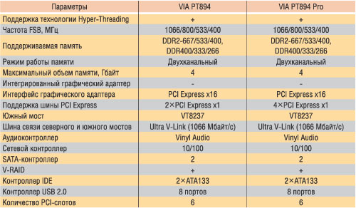
Via PT894.
The VIA PT894 chipset became the first VIA chipset with full support for the PCI Express X16 interface. The northern bridge of this chipset supports the frequency of FSB 1066/533/800 MHz, and a two-channel memory controller supporting the VIA STEPUP technology allows you to use the memory of the DDR2-667 / 533/400 or DDR400 / 333/266 standard, and the memory slots of different standards may be Installed on the motherboard at the same time. In addition to the PCI Express X16 tire, the North Bridge of the VIA PT894 chipset supports two more PCI Express X1 channels. The Northern Bridge VIA PT894 is designed to work with the South Bridge of VT8237, to communicate with the Ultra V-Link bus with a capacity of 1066 MB / s.
Since the interaction of the Northern and South Bridges chips is about the interaction of the Northern and South Bridges, it is worth mentioning the V-MAP technology (VIA modular architecture platform) implemented by VIA for the specified system of system logic chip, and this means that, in principle, the VT8237 chip place can Success to occupy another version of the southern bridge, made in accordance with V-MAP technology. True, it is only a theoretical possibility, and in practice now traditional is the bunch of chips VIA PT894 and VT8237. Speaking about the capabilities of the Northern Bridge PT894 chip, it is necessary to mention the technology of Via FastStream64 Technology, implemented in this chip and designed to reduce the latency of the memory controller, for which an enlarged prefetch Buffers is used. Thus, according to the manufacturer's assertion, it is possible to achieve an increase in performance with a smaller number of transistors of the northern bridge than when implementing two-channel memory access.
The southern bridge has a built-in two-channel IDE controller that supports the IDE devices to the ATA33 / 66/100/133 or ATAPI interface, as well as a SATA controller that supports the operation of two SATA 1.0 ports and the SATALITE interface that when using an optional SATALITE interface controller. Allows you to maintain the work of two SATA ports. The built-in V-RAID controller makes it possible to organize SATA disks in the RAID array of levels 0, 1 and 0 + 1 (the last mode is possible only when the four SATA devices are connected).
We also note the presence of a built-in network controller FAST Ethernet, a USB 2.0 controller with support for eight ports and support up to six PCI slots. The AC'97 digital controller with Vinyl Audio technology provides the ability to implement both sound 5.1 when using the 6-channel AC'97 codec and eight-channel audio of format 7.1, for which the VIA VINYL GOLD AUDIO 7.1 controller is required.
VIA PT894 PRO.
The difference between the VIA PT894 Pro chipset from VIA PT894 is that the VIA PT894 Pro chipset supports DualGFX Express technology. The essence of this technology is as follows: in the VIA PT894 Pro model there are 20 PCI Express X1 channels, of which 16 are used for the PCI Express X16 interface, and 4 more - for the PCI Express X4 interface, but in the PCI Express X16 form factor. Thus, on motherboards based on the VIA PT894 Pro chipset, there are two PCI Express X16 slots, which allows you to simultaneously install two video cards with the possibility of organizing the mode like SLI, but according to the PCI Express X16 + PCI Express X4 scheme.
In all the rest of the VIA PT894 Pro chipset is identical to Via PT894.
VIA chipsets for AMD processors
The modern range of chipsets for processors with AMD64 architecture (Table 8) includes four models: Via K8M800, VIA K8T800, VIA K8T800 Pro and Via K8T890, but only two models (K8T890 and K8M890) support the PCI Express X16 interface.
It is characteristic that in VIA chipsets for processors with AMD 64 architecture, the same southern bridge (VIA VT8237) is used as in Intel processors, and this has become possible due to the use of the universal V-LINK bus connections of the northern and southern bridges, as well as using V-MAP technology.
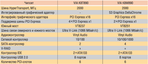
Via K8T890.
Today, the VIA K8T890 chipset is the only solution from VIA for AMD64 processors with PCI Express tire support, that is, the chipset can be positioned for the most productive systems, game PCs and graphics stations. The optimal is the combination of this chipset with AMD Athlon 64 FX and AMD ATHLON 64 X2 Dual-Core processors.
The North Bridge of the VIA K8T890 chipset combines the Hypertransport bus interface with a clock frequency of 2000 MHz to communicate with the processor, as well as the Ultra V-LINK bus interface with a capacity of 1066 MB / s; Through this tire is interacted with the southern bridge.
In addition, the North Bridge VIA K8T890 supports the PCI Express X16 bus to install an external video card, as well as four more PCI Express X1 lines.
Via K8M890.
The VIA K8M890 chipset is the newest chipsets with the built-in graphics core (Integrated Graphics Processor, IGP) for processors with AMD64 architecture. Unlike the VIA K8M800 chipset, the VIA K8M890 uses the graphics core S3 Graphics Deltachrome of a new generation that implements the DirectX 9 hardware support that supports the pixel shaders version 2.0 and having two pixel conveyors. The nucleus clock frequency is 250 MHz. In addition, S3 Graphics Deltachrome supports all HDTV formats, including 1920-11080.
To communicate the VIA K8M890 chip with the processor, high-speed Hypertransport interface with a clock frequency of 2000 MHz is used.
In order to install an external video card in the VIA K8M890 chip, the PCI Express X16 interface is provided, and to support extension cards there are two more PCI Express X1 lines.
The Northern Bridge VIA K8M890 is used in a bundle with the new South Bridge VT8251, and the Ultra V-Link tire with a bandwidth of 1066 MB / s is used to communicate the Northern and South Bridges.
The South Bridge VIA VT8251 in its functionality exceeds its predecessor - the chip VT8237. First, a four-channel SATA II controller has been added with the possibility of combining disks in RAID arrays of levels 0, 1, 0 + 1 and 5, and secondly, two PCI Express X1 lines and a gigabit network controller (MAC level) are added.
ATI chipsets
about compared with such market leaders, like Intel, Via, Sis and Nvidia, ATI can hardly be classified as large players in the chipset market for desktop systems. Actually, the range of chipsets manufactured by ATI is still quite modest, and the manufacturers of motherboards are not in a hurry to announce the models based on ATI chipsets.
The modern ATI chipset model range is not too large and includes only several ATI Radeon Xpress 200 series chipsets, but in two versions - for AMD processors and for Intel.
ATI chipsets for Intel processors
The ATI chipset model range for Intel processors is still quite small, and if we talk about modern chipsets, then there are only two of them - ATI Radeon Xpress 200 for Intel Processor (RS400 code name) and ATI Radeon Xpress 200 Crossfire Edition for Intel Processor (RD400).
ATI Radeon Xpress 200 for Intel Processor
The name of the chipset (for Intel Processor) suggests that this chipset is intended for Intel processors. Actually, differences in functionality between ATI Radeon Xpress 200 and ATI Radeon Xpress 200 for Intel Processor are minimal, but the northern bridges of these chipsets differ significantly from each other.
The North Bridge of the ATI Radeon Xpress 200 for Intel Processor chipset bridge combines the FSB bus interface with a clock frequency of 533/800 MHz (the frequency of 1066 MHz is also unofficially supported). Accordingly, the chipset supports the processors of the Intel Celeron D family, Intel Pentium 4 and Intel Pentium 4 Extreme Edition (Intel Pentium D dual-core processors are not supported).
The two-channel controller integrated into the northern bridge supports DDR2 400/533/667 memory with a maximum up to 4 GB. In addition, the North Bridge ATI Radeon Xpress 200 for Intel Processor supports the PCI Express X16 bus to install an external graphics card and has four PCI Express X1 lines. Naturally, the chipset's northern bridge is integrated by the ATI Radeon X300 graphics core. However, supporting HyperMemory technology in the ATI Radeon Xpress 200 for Intel Processor chipset is not implemented, that is, a selected personnel buffer in the form of a separate chip on the motherboard is missing.
The South Bridge of the IXP400 of the ATI Radeon Xpress 200 for Intel Processor chipset is exactly the same as in the AMD64 processor version, and includes support to seven PCI slots, up to four SATA devices with the possibility of organizing two independent RAIDs levels of levels 0 and 1, up to eight USB 2.0 ports and up to four devices (two channels) ATA133. In addition, AC'97 audio controller is integrated in the Southern Bridge.
ATI Radeon Xpress 200 Crossfire Edition for Intel Processor
ATI Radeon Xpress 200 CrossFire Edition for Intel Processor, known for the RD400 code name, is an ATI Radeon Xpress 200 for Intel Processor chipset, but with support for CrossFire technology, which implies the ability to combine two video cards to increase productivity. In Systems based on ATI Radeon Xpress 200 Crossfire Edition for Intel Processor, there are two PCI EXPRESS X16 slots, but each of them uses the PCI Express X8 bus. Thus, in the ATI Radeon Xpress 200 CrossFire Edition For Intel Processor chipset, one PCI Express X16 bus is divided into two PCI Express X8 tires.
There is another insignificant difference of the ATI Radeon Xpress 200 for Intel Processor and ATI Radeon Xpress 200 CrossFire Edition for Intel Processor: In the last of them, the South Bridge is iXP450, which is fully compatible on the interface and on wiring with the IXP400 bridge.
The difference between IXP400 and IXP450 is that High Definition Audio support has been added to the IXP450 instead of the obsolete AC'97 interface.
ATI chipsets for AMD processors
ATI chipset model range for AMD processors (Table 9) is also still quite modest and is presented in three models of the ATI Radeon Xpress 200 family.
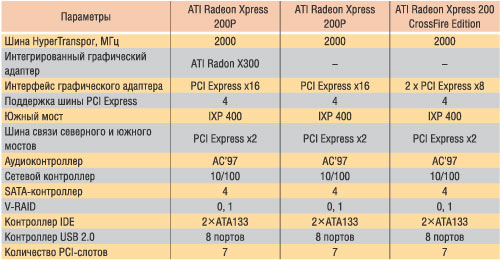
ATI Radeon Xpress 200p (RS480)
ATI Radeon Xpress 200p (RS480 code name) is a modern chipset of a classic two-seater structure with a built-in graphics controller for platforms based on the processor with AMD64 architecture.
The RS480 north bridge combines the Hypertransport bus interface with a clock frequency of 2000 MHz to interact with the processor, the PCI Express X16 bus interface for installing an external video card, four separate PCI Express X1 lines, as well as the interface of the interaction of the northern and southern bridges. Note that in this case, the PCI Express X2 bus is used.
The Radeon Xpress 200 graphics core is based on the ATI Radeon X300 kernel (option Radeon 9600 under PCI Express), that is, hardware supports DirectX 9, including vertex / pixel programs 2.0. The kernel possesses two pixel conveyors with one textural unit for each, as well as four vertex blocks. The frequency of the graphics core is 350 MHz.
ATI Radeon Xpress 200P feature is HyperMemory's branded technology - this is the possibility of organizing frame buffer in a dedicated system of system memory (traditional approach for integrated graphics controllers) or isolation under the personnel buffer of special memory (up to 128 MB), which is integrated as a separate chip or chip on the motherboard.
Of the additional features of the integrated graphics core, you can note the support of the image output into two independent monitor, and in conjunction with the external graphics card, the output to three monitors is supported.
In combination with the North RS480 bridge, the South Bridge of the IXP 400 is used, which supports up to seven PCI slots, up to four SATA devices with the ability to organize two independent RAID arrays of levels 0 and 1, to 8 USB ports 2.0 and up to four devices (two channels) ATA133 . In addition, AC'97 audio controller is integrated in the Southern Bridge.
ATI Radeon Xpress 200 (RX480)
ATI Radeon Xpress 200 (RX480) is analogous to the already considered ATI Radeon Xpress 200P chipset, but not having a built-in graphics core.
ATI Radeon Xpress 200 Crossfire Edition (RD480)
ATI Radeon Xpress 200 CrossFire Edition, known as the RD480, is an ATI Radeon Xpress 200 chipset version, but with support for CROSSFIRE technology. In fact, the difference between the ATI Radeon Xpress 200 Crossfire Edition and ATI Radeon Xpress 200 chipsets is the same as between NVIDIA NForce4 SLI and NVIDIA NForce4 Ultra chipsets.
In the Systems based on the ATI Radeon Xpress 200 CrossFire Edition XPress 200 CrossFire Edition edition, the PCI Express X16 bus is divided into two PCI Express X8 tires, but the video cards are set to install the PCI Express X16 interface.
There is another minor difference of ATI Radeon Xpress 200 chipsets and ATI Radeon Xpress 200 Crossfire Edition: The last IXP450 south bridge is used, which is fully compatible with the interface and wiring with the IXP400 bridge.
ULI chipsets
uLI IPSETs occur very rarely, and mainly in budget parents for PCs or laptops. In addition, although the range of these chipsets is not too large, there are chipsets for both AMD64 processors and Intel processors. The characteristic feature of the ULI chipsets is the possibility of using a northern bridge with various southern bridge options, which is ensured by the universal bus interface of the southern and northern bridges. In addition, the Northern Bridges of Intel and AMD processors are combined with the same southern bridges. Often you can meet a combination (sort of hybrid chipset) of the North ATI bridge with the South ULI Bridge.
ULI chipsets for AMD processors
The modern range of ULI chipsets for processors with AMD64 architecture consists of only two models: ULI M1689 and ULI M1695.
ULI M1689.
ULI M1689 is a single-chip solution for platforms based on processors with AMD64 architecture (Socket 940/745/939). The ULI M1689 chip is integrated AGP 8X controllers, a two-channel IDE controller ATA133, a USB 2.0 controller with support for up to eight ports, an Ethernet 10/100 network controller (MAC level), as well as a two-channel SATA controller and a Hypertransport tire controller that connects the chip with processor. Note that the Hypertransport bus supports the clock frequency of 2000 MHz, which allows the use of the ULI M1689 chip with the most modern AMD processors at Athlon 64 and AMD Athlon 64 FX with a two-channel memory controller. However, given the positioning of the ULI M1689 chip, it is optimal to consider its combination with the AMD Sempron processor.
The sound subsystem integrated into the ULI M1689 chip is a 6-channel and based on an AC'97 controller.
ULI M1695.
The model ULI M1695, which, unfortunately, has not received widespread, is unique in its kind chipset and does not have competitive analogues. The ULI M1695 chipset is designed for high-performance ATHLON 64 and AMD ATHLON 64 FX families (Socket 754/940/939) with a two-channel memory controller.
ULI M1695 chipset bridge, which ULI terminology is called Hypertransport PCI Express Tunnel Chip, connects the PCI Express X16 bus controller, which can be configured as PCI Express X16 or as two PCI Express X8 tires with the possibility of combining two video cards (analog NVIDIA NFORCE4 SLI ). In addition, ULI M1695 supports four more PCI Express X1 lines, which can be configured as two PCI Express X2 tires or as one PCI Express X4 bus.
To communicate ULI M1695 with the processor, the standard Hypertransport bus with a clock frequency of 2000 MHz is used. In addition, exactly the same universal tire is also used for the connection of the Northern Bridge with a south bridge or with any other chip that supports this interface.
Thus, the ULI M1695 provides parent-maternal manufacturers with sufficient flexible capabilities to configure various options for using the chipset.
A typical combination is the Northern Bridge ULI M1695 and the South Bridge ULI M1567. In addition to standard interfaces (two ATA133 ports, two SATA ports, eight USB 2.0 ports, AC'97 audio, 32-bit PCI bus and Ethernet controller) South Bridge ULI M1567 contains a full-fledged AGP8x interface. Note that there are solutions that support the PCI Express X16 and the AGP interface simultaneously. However, as a rule, we are talking about pseudo-AGP, which is implemented via the PCI bus and has low bandwidth. In this sense, the ULI M1695 / M1567 solution has no analogues.
ULI chipsets for Intel processors
Today's model range of ULI chipsets for Intel processors consists of two models: ULI M1683 and ULI M1685, built according to the classic two-seater.
ULI M1683.
The ULI M1683 chipset is designed for systems based on the Intel Pentium 4 family processors, as well as for mobile processors of the Intel Pentium M.
The ULI M1683 north bridge contains a single-channel memory controller that supports DDR266 / 333/400 or PC133 SDRAM memory with a maximum up to 4 GB. The system tire controller supports the frequency of FSB 800/533/400 MHz. In addition, to install an external video card in ULI M1683 there is an AGP8X / 4X interface.
To communicate with the south bridge, a universal Hypertransport bus (800 MHz, 8/8 bits) with a bandwidth of 1.6 GB / s is used. As a southern bridge, in combination with ULI M1683, the ULI M1563 chip can be used, in which the ATA133 two-channel controller is integrated, USB 2.0 controller with support for up to six ports, 32-bit PCI bus controller, network Ethernet controller and traditional audio controller based on AC '97.
ULI M1685.
Model ULI M1685 is focused on a budget solution - the processors of the Intel Pentium 4 family and mobile processors Intel Pentium M.
The ULI M1685 north bridge includes a single-channel memory controller that supports DDR266 / 333/400 or DDR2-400 / 533/400 or DDR2-400 / 533/667 memory with a maximum volume of up to 3.5 GB. The system tire controller supports the frequency of FSB 800/533/400 MHz.
It should be noted that the North Bridge ULI M1685 supports the PCI Express X16 graphical interface, which allows you to position this chipset as a basis for mid-level systems.
To communicate with the southern bridge in the ULI M1685 chipset, a universal Hypertransport bus with a clock frequency of 1600 MHz and with a 1,6 GB bandwidth is used. As a southern bridge, any chip of the ULI M15xx family can be used, but the optimal is the combination of ULI M1685 with ULI M1566. The functionality of the South Bridge ULI M1566 is characterized by PCI Express Tire Support (one PCI Express X4 port or two PCI Express X1 ports), as well as the presence of a two-channel SATA controller.
South Bridges ULI M1573 / M1575
Unlike other companies engaged in the production of chipset, ULI manufactures universal options for southern bridges, compatible with the northern bridges of other manufacturers. In particular, the South Bridge ULI M1566 turned out to be the last chip in which the Hypertransport bus was used to connect to the North Bridge. The new generation of southern ULI bridges (ULI M1573 / M1575 chips) uses a more versatile bus - PCI Express for this purpose. Replacing the Hypertransport Connection on PCI Express opens up broader opportunities for combining southern ULI M1573 / M1575 bridges with northern bridges of other manufacturers. In particular, the integrated ATI chipsets can be complemented by these southern bridges.
According to the functionality, the South Bridges ULI M1573 / M1575 exceed the capabilities of the M1563 and M1566 chips. Thus, in the ULI M1573 chip, a four-channel SATA controller is integrated with the possibility of creating Raid arrays of levels 0, 1 and 0 + 1, support for eight USB 2.0 ports is implemented, and in addition, the High Definition Audio sound controller is integrated. To communicate with the North Bridge in the ULI M1573 chip, the PCI Express X2 bus is used.
The ULI M1575 chip is somewhat superior to the functionality of ULI M1573. For example, a Tire PCI Express X4 is used to communicate with the northern bridge. In addition, the ULI M1575 chip is equipped with a four-channel SATA II controller with the possibility of creating RAID arrays of levels 0, 1, 0 + 1 and 5.
In addition, the ULI M1573 / M1575 chips are characterized by a reduced level of energy consumption, which creates prerequisites for their use in mobile platforms.


